Four Options Tailored for Your Needs
We offer four levels of process complexity that can be adapted for a wide range of uses. We can process 4" (100 mm) and 6" (150 mm) wafers. We are happy to integrate our process into another process flow or work with a customer to put their unique material or structures onto a custom piezoMEMS device. Our goal is to give our customers the maximum level of flexibility in realizing their design.

Global Films
This package provides you with the base essentials for you to be able to build your own device.
- Pattern and etch your own structure of choice
- Platinum electrodes
- Sol-gel lead zirconate titanate (PZT)
- Gels made in house
- Custom doping (Nb, La, etc.); compositions from paraelectric, morphotropic phase boundry, to antiferroelecric and everything in between; and interfacial layers are available
- On Silicon or Silicon on Insulator substrates
- Great for researchers with access to fabrication facilities

Unencapsulated Clamped Devices
The simplest testable device that we offer.
- Patterned version of our Global Films
- Good for integration into more complex device stacks and aligned with sensors, filters, or other structures
- Great for laboratory/probe-station use
- Three pattern layers: Pt bottom electrode, Pt top electrode, PZT etch to clear field and open vias
- Optional 4th layer can add solder or wire-bond pads
- On Silicon or Silicon on Insulator substrate
- Can be delivered as a full wafer for further processing or diced

Encapsulated Clamped Devices
More robust. Longer shelf life. Better long term reliability.
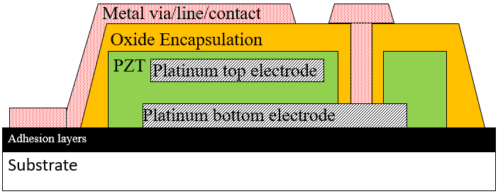
- Builds upon Unencapsulated Clamped Device
- Great for installation into larger systems or remote applications
- Good for applications where you may not have direct access to the system
- This type of device serves as reference capacitor in our testers
- Added oxide encapsulation for improved reliability
- Metal vias, conductive lines, and contact pads
- On Silicon or Silicon on Insulator substrates
- Can be packaged by soldering or wire bonding for easy integration onto a circuit board.
- Can be delivered as a full wafer for further processing, diced, or packaged

Encapsulated Unclamped Devices
When you need large displacements. Motion on the micrometer scale.
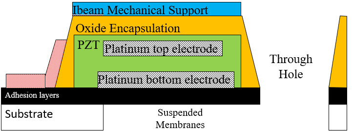
- Builds on Clamped Encapsulated Device
- Enables cantilevers, diaphragms, and other structures to have micrometer scale displacements
- Added metal I-Beam mechanical support layers provide strength to released membranes
- Additional etches open through holes and release membranes.
- On Silicon, or Silicon on Insulator substrates
- Delivered as released individual die or die-on-PCB
